Create highly integrated products with a smaller package and increased functionality
Semiconductor industry demands for higher levels of integration and lower costs coupled with a growing awareness of complete system configuration have continued to drive the popularity of System in Package (SiP) solutions. Amkor’s SiP technology is an ideal solution in markets that demand a smaller size with increased functionality. By assembling, testing and shipping millions of SiP devices per day, Amkor Technology has a proven track record as the industry leader in SiP design, assembly and test.
Amkor’s Center of Excellence for substrate-based SiP technology is located in our largest volume manufacturing facility in ATK4 Kwangju, South Korea. The large-scale manufacturing capabilities in ATK4 factory can achieve significant volume production support with very high yields with short cycle times.
Amkor Technology defines advanced SiPs as multi-component, multifunction products in an IC package. They require high-precision assembly technologies, which leverage Amkor’s strengths.
- Size reduction
- Ultra-thin package
- Thin substrate with core and coreless using finer line and spacing
- Conformal and compartmental shielding
- Low filler size for mold underfill
- Fine pitchflip chipandcopper pillar
- Double side assembly
- Test developmentand production test
- Turnkey solution

系统方案技术允许多个等优点ced packaging technologies to be combined to create solutions customized to each end application. Laminate based SiP technology is in a front-runner solution and most popular SiP solution for cellular, IoT, power, automotive, networking and computing system integrations.
Existing market uses for SiP include:
- RF and wireless devices
Power amplifiers, front-end module, antenna switch, GPS/GNSS modules, cellular handset, and cellular infrastructure, Bluetooth®solutions, 5G NRAntenna in Package(AiP) - IoT for wearable and Machine to Machine (M2M)
Connectivity,MEMS, microcontroller, memory, antenna, PMIC and other mixed-mode devices - Automotive applications
Infotainment and sensory modules
- Power modules
DC/DC converter, LDO, PMIC, battery management and others - Logic, analog and mixed-mode technology
Tablets, PCs, display and audio - Computing and networking
5G networking and modems, data center, storage and SSD - Extension of the technology platform to a wider field of application areas is ongoing
Antenna in Package (AiP)/Antenna on Package (AoP)
(5G NR) SiP Solutions
Millimeter wave (mmWave) radio design with beamforming and array antenna will be used in varieties of advanced SiP products for 5G cellular systems. Millimeter electromagnetic wave design is imposing a new challenge for the system designers, components and SiP packaging engineers.

Key Amkor Packaging Technologies for AiP/AoP
- Greater than 26 GHz achieved
- Compartmental shielding
- Partial (selective) conformal shielding
- Partial molding
- Body size: up to 23.0 mm x 6.0 mm
- Substrate layer counts: up to 14 layers
- Low loss and low dielectric substrate
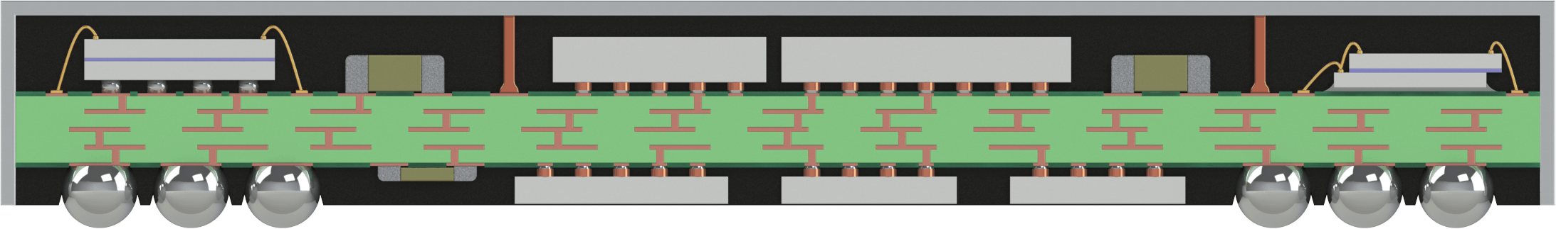
Double Sided Molded Ball Grid Array (DSMBGA)
To further improve the integration and robustness of RFFE solutions, Amkor has developed a Double Sided Molded Ball Grid Array (DSMBGA) package to allow molded assembly of components on both sides of the substrate.
 Key Amkor Packaging Technologies for DSMBGA
- Increased integration for RFFE modules with significantly reduced package height
- Allows integration of antenna tuners and passive components
- Improves signal integrity and reduces losses
- Conformal and compartmental shielding for EMI isolation
- In-line RF testing
DownloadDSMBGA Data Sheet
Questions?
Contact an Amkor expert by clicking the request info button below.