Semiconductor Tales: The Start of a Package, Vol.1
Designing a Package
Hello to all dear readers of Amkor In Story, this is Gyuik Jeong. As the new writer of Semiconductor Tales, I will be continuing the story anew in 2017. I entered the company as part of the Design Team and worked on design business activities for about six years. I had no idea what a semiconductor package was before starting. But with help from many good folks, I progressed from knowing nothing about packaging to understanding a lot about packages in general. So, my first topic will be package design.
The dictionary definition of ‘design’ is planning and deciding the structure, each material, shape, size and more for producing a machine, apparatus or other equipment. Since the beginning of the semiconductor packaging industry, many kinds of package products have been developed. Today’s topic, design, is about choosing one of the products and design appropriately for it.
Personally, I think the first step in design is choosing the kind of package. From the number of required input/output (I/O) terminals, size and shape of the package, electrical and thermal properties, to the most important one – the price, many conditions must be considered thoroughly to choose the most suitable product. The decisions can occur before designing, but sometimes can be changed later due to the aforementioned reasons.
Substrate Design
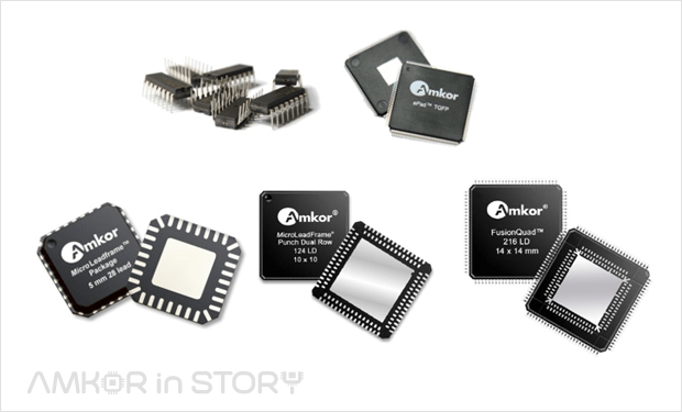
The second step is designing the substrate. One of the criteria to distinguish between package types is about which substrate to use. The traditional choice is a leadframe, which is wiring through etching on a copper plate. It’s relatively cheap, and has advantages in electrical and thermal properties, so many products continue to use it. However, the number of required I/O sockets keeps growing as semiconductor chips incorporate more and more functions, and we reached the structural limitations of leadframe packages. Since it has I/O sockets only on the outside of the package, to have more sockets, the package has to get bigger. As shown in the picture below, two or three lines instead of one and different shapes of I/O sockets can be used but the leadframe still has difficulty meeting all the needs. Also, designing with it can often be difficult because only one wiring layer can be used.

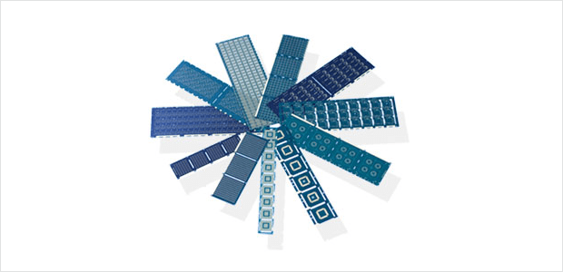
You might have heard of ‘PCB’ even if you don’t work with semiconductor packaging. PCB stands for printed circuit board, and can solve many of the disadvantages of the leadframe. Let’s take a look at the simplified structure.
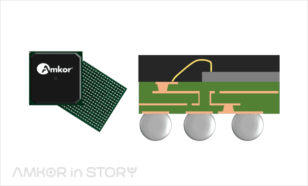
基本结构电绝缘垫erial in between conductive layers that are designed appropriate to the purpose. Since it is a bit hard to explain in words, look at the picture below. A leadframe has limitations of wiring design, so for wire bonding, it must use the nearest lead pin. If you want to connect to a pin on the other side, like the red one in the picture, it is not impossible per se, but it can be problematic in processing or result in a compromise in the package’s performance. Today, PCBs can use multiple wiring layers and Vias for vertical connections between layers to easily connect where you want. (Continued in the next issue.)
WRITTEN BY Gyuik Jeong
It is already 10 years since my ambitions lead me to Amkor. They say 10 years is enough to change the face of the earth, but I wish for my mind to stay curious and amazed at each and every work like a new recruit, so the work is always enjoyable.
Related Posts

A Look Inside ADAS Modules

Is There Hope for Auto Semis?