Increasing the Conductive Density of Packaging
Wide bandgap (WBG) semiconductor technologies have created new challenges and opportunities for power packages. Developments such as silicon carbide (SiC) and gallium nitride (GaN), have a higher figure of merit (FOM) compared to silicon MOSFETs and have extended the efficiency, output power and/or switching frequency range and operating temperature range for power electronics.
With lower losses, a given size power device can control higher power loads. For example, with GaN power transistors, a power system can have ¼ the size, weight and efficiency losses compared to a silicon-based system. GaN technology can solve the system challenges from the low power (50W) end to medium and even high-power levels in wireless systems and more. Its acceptance in 5G applications makes it well-positioned for sophisticated low to medium power packaging. Similarly, SiC has power control capabilities beyond those of Si MOSFETs and requires advanced packaging for many applications. The gains and advantages in WBG devices need new packaging options to maximize the value of the entire power system.
Today’s discrete power packages are limited to the electrical performance of clip, wire and solder interfaces. In general, discrete packaging follows the design philosophy that greater size/volume correlates to higher power handling capability. However, these more efficient transistor technologies provide the ability to handle more power in the same size package or to reduce the form factor significantly.
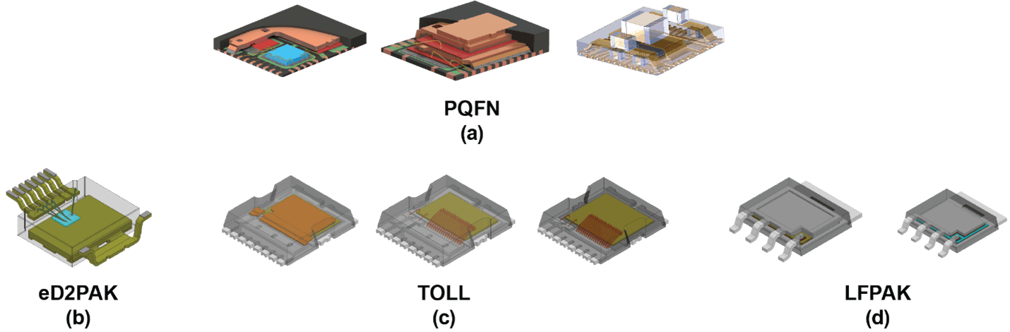
Figure 1.Available power discrete capabilities include(a)PQFN evolution,(b)eD2PAK with heat spreader tab,
(c)TOLL variations and(d)LFPAK.
To maximize the total conductivity in traditional power packaging, the source and drain need to be connected to current carrying materials at or near 100% of the available space in the die design. Traditionally, this is done by increasing the number of wires, increasing the wire diameter, or maximizing the size of the clip attached to the source or drain.
从根本上改善电力sp的功能ace, three things must occur. First, the total conductivity from source and drain needs to be maximized. Second, thermal and electrical interfaces need to be eliminated or considerably reduced in length/thickness. Third, the conductive material density of the package needs to be increased. In the below figure, we examine the conductive density across a wide range of power-specific packaging in use today.
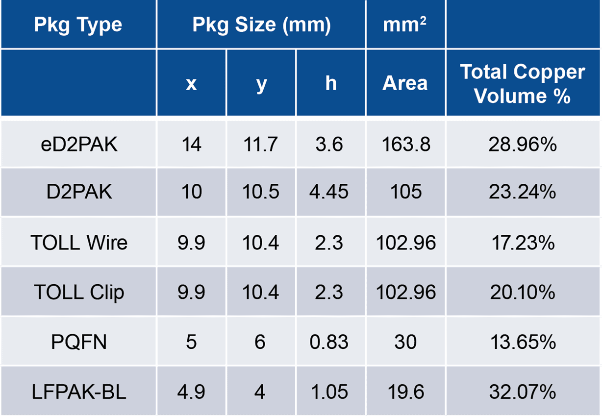
Table 1.Comparative data on existing power packages.
To maximize both the thermal and electrical properties, it would be preferred to have as much conductive material as possible within the volume of the package. In most power packaging today, the conductive material in the package rarely goes above 25% (refer to Table 1).
New package formats need to be created to maximize conductive density in the package. One concept is the PowerCSP™ technology developed by Amkor. PowerCSP technology is typically in the 40-70% range for conductive density and can be designed in a much smaller form factor than traditional power packages as a result. This increase is due to the use of a continuous Cu substrate instead of a clip or wires.
 Figure 2.Implementation of PowerCSP™ technology shows its flexibility and many construction options.
In the PowerCSP technology, designs allow the die to use all the available source and drain area by connecting the die directly through a Cu pad that serves both as the current-carrying and heat-dissipating element. This results in lower resistance and inductance for the package compared to the group. Total package conductive density plays a factor, and also the use of the entire interface for source and drain to minimize potential losses in the system.
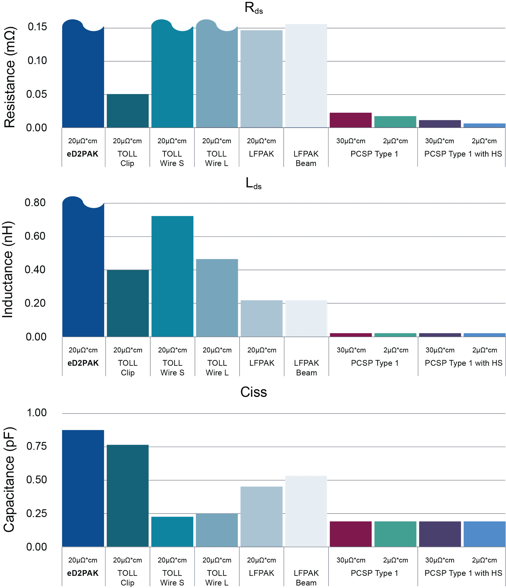
Figure 3.Simulated comparison of RDS, LDS and Ciss for the PowerCSP™ (PCSP) design to different versions of eD2PAK, TOLL and LFPAK packages.
Other package concepts might be developed specifically for power, but the conductive density of the package will be a key factor. Whether it is Si, GaN or SiC, all can benefit from increasing the conductive density of the package to lower resistance, inductance, and to ultimately reduce the form factor of the package itself. Efforts to increase the conductive density of the package can only help to address the overall power density of the package and allow us to take advantage of all that Si and WBG devices have to offer.
About the Author
Shaun Bowers is VP, Mainstream Advanced Package Integration at Amkor Technology Inc., Tempe, AZ. He joined Amkor in 2000 and is currently responsible for package development in automotive, leadframe and power packaging business segments. He previously held technical program management, sales and customer service roles as well. Prior to joining Amkor, he worked for Johnson Matthey Electronics and Honeywell Electronic Materials. He holds a degree in Mechanical Engineering from Gonzaga U.
Related Posts

Meeting the Challenges of 5G RF Production Test Services
Amkor Technology China Recognized By GOODIX Technology, Inc.