48V Ecosystem and Power Packaging Trends

随着每年通过的,新兴增长应用领域如Automotive, Cloud Computing,工业Automation, and Telecom (5克) Infrastructure are garnering more attention. Although the application segments are different, there is a commonality in how voltage conversion and power distribution are achieved at the system level. System demands are becoming more important to reduce an effective carbon footprint. As a result, a new 48V Ecosystem is being developed and deployed to meet various objectives, including very high efficiency. Whether its power supplies, computing elements or memory blocks, semiconductors are at the crux of the solution in meeting these demands. The focus of this paper is to discuss market and technology trends in each of these application areas and share thoughts on how innovative power packaging platforms are trying to meet both electrical and thermal requirements.
Automotive
今天大多数奢侈品车辆运行数百万线代码网络,最多100个电子控制单元(ECU)[1]。在汽车中的电气化,舒适性和先进的驾驶员辅助系统(ADA)越高,对总功率预算的需求越高。作为这些先进功能的一些,今天在豪华车迁移到标准汽车时,成本变得迫切,而不会牺牲电力系统的效率。今天现有的车辆电源树直接从12V电池供电,以便机械辅助载荷(通常<5-7 kW),如水和油泵,气候压缩机,主动滚动控制,前灯和尾灯。这些负载结合了满足企业平均燃料经济性(咖啡厅)标准和富力耗能的ADAS系统的额外要求,以满足企业平均燃料经济性(CAFE)标准和耗电的ADAS系统,使其充满努力提高效率。虽然汽车原始设备制造商(OEM)已经用电气对应物更换机械驱动的部件多年,但还需要进一步需要48V系统等较新的架构。在短期内,OEM及其第一(Tier1)供应商可以选择双重架构(12V和48V),直到将来发生永久转换到48V电网。
汽车OEM和TIER1最近推出了几种轻度混合动力电动汽车(MHEV)解决方案。例如,奥迪推出了一种新的带式交流发电机系统(BAS),其容量为12千瓦,为其轻度混合动力汽车提供动力,同时还为传统的12伏系统安装了DC-DC转换器[2]。同样,戴姆勒也为其S级引入了一款集成启动发电机(ISG),容量高达16千瓦[2]。戴姆勒和奥迪一样,也在为传统的12V负载安装DC-DC转换器模块。Tier1供应商Valeo推出了其eCruise4u平台,将自动驾驶和48V混合动力系统结合在一起。作为该平台的产品之一,e4AWD巧妙地结合了集成式皮带起动发电机(iBSG)和电动后桥驱动(eRAD),为其MHEV系统增加了22kw的容量,从而降低了17%的燃油消耗。德尔福,另一个汽车Tier1,已经推出了一个48V混合动力系统,如图1所示,其中包括一个电子增压器,提高燃油效率15%。这个电子增压系统还可以使用动态跳过火(DSF)缸停用的概念,减少13%的二氧化碳排放量[2]。
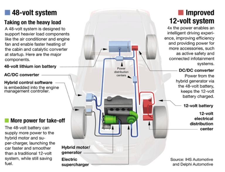
图1:来自Delphi Technologies的48V温和混合动力系统(以前的Delphi Automotive)
转换到48V电源网可以实现多种益处,例如布线线束横截面和减轻重量,导致较轻的车辆和减少减少。虽然在转向架中的机械部件的电气化,舒适性和便利性和其他系统有助于,使用电机(<25kW)温和杂交将具有显着的有形效果。一个估计表明,MHEV将使二氧化碳排放量减少15%,其中大约为全混合系统成本的大约30%的益处的70%。显然,预计与全杂化车约4500美元相比支付额外1500美元左右的支付1500美元左右的愿意为MHEV车辆增长产生动力。此外,48V电源网还可以用于为未来的车辆到所有(V2X)连接和ADA提供系统准备(负载控制点)。在未来十年期间,随着3级到5级的自动驾驶车辆,ADAS系统的电源要求将仅涌现。目前的2级能力按1KW的顺序需要功率速率,而4级/级5系统需要10倍的电力。这与成本和排放福利一起,48V MHEV系统被视为扩张EV市场的网关。
Cloud Computing
如今,全球需要700多万个数据中心来管理每天从个人和商业用途创建的超过25亿字节的数据。在迄今为止已创建的44 zettabytes(44万亿千兆字节)数据中,90%的数据是在过去2年中创建的[3]。由于OTT流媒体服务、5G、物联网的出现(IOT.), and social media, big data is expected to morph cloud and edge datacenter markets significantly. A typical data center would offer services such as data storage, processing,联网, and distribution. To manage these services, operators require tremendous amounts of power on the order of several 100s of MW. As much as 40% of the operating costs of the data center comes from the energy needed to power and cool racks of servers [4]. Power Usage Effectiveness (PUE) and Total Cost of Ownership (TCO) are two very important metrics for data center operators to reduce costs and improve utilization. On average, approximately 30-35% of the power is wasted in the conversion from the AC grid to the microprocessors of an individual server. Along this power path, losses can be reduced mainly in three areas – universal power supply (UPS, grid-to-data center), server rack power supply, and individual server power supplies. Until a few years ago, data centers were designed for 4 to 5kW per rack and now they are up to 10kW per rack. Increasing rack power density up to 30kW or more will be the trend in the future [5]. As a result, smaller and efficient power supplies are needed as they can improve the PUE, resulting in greater server density and additional revenue per foot of floor space ($/ft).
图2:数据中心电源输送系统(源:Wiwynn [5])
In terms of power architecture, current data centers are designed to the 12V power net as shown in Figure 2. Like the automotive 48V system, datacenters’ power architecture also supports the shift to 48V. The shift results in higher power density, lower distribution losses (I2R losses by 16X), higher efficiency, deployment flexibility, and cost-effective in-rack UPSs [5]. The benefits at the rack level are obvious, given the reduction in busbar sizing, number of turbo capacitors, and copper losses. However, the challenge remains on how to achieve the voltage conversion from 48V to the server board. To power up the central processing unit (CPU) cores and Double Data Rate (DDR) memory blocks, traditionally sub 1.8V is required. For a higher step-down ratio (48V to 1.8V), achieving similar conversion efficiencies of switching circuits is difficult. Each power conversion stage, including AC-DC and DC to point of load, must have similar or higher efficiency at the rack level. To meet the system level congruity, smaller form factor and higher power capable semiconductor packaging are key.
5克Infrastructure
为了解决当前4G网络的缺点,5克networks应该能够处理大量流量(无线电)和大容量(IoT,连接密度和带宽),同时非常可靠(边缘计算,延迟)。关键的变化包括新的频谱,更多的网站和多访问边缘计算。目前,4G LTE网络的传输带宽的理论极限约为150 Mbps,其无法满足5G的要求。为了实现更高的带宽,5G网络使用较高的C波段。此外,大规模多输入多输出(MIMO)技术是提高吞吐量的关键。如图3所示,就拓扑而言,现有的4G网络赞成分布式无线电接入网络(DRAN)架构,其中天线,远程无线电头(RRH)和基带单元(BBU)是分开的。然而,5G网络倾向于赞成集中式或云(C-RAN)分发以整合基带功能,将它们从小区站点移动到集中位置。在5G网络中,预计RRH和天线是集成的,而BBU池位于边缘站点。BBU池(或核心网络)共享相同的物理基础架构,包括路由器,物理基础设施,电力和冷却系统等网络设备。然而,更多的网站和更高的计算要求将进一步提高网络能耗。
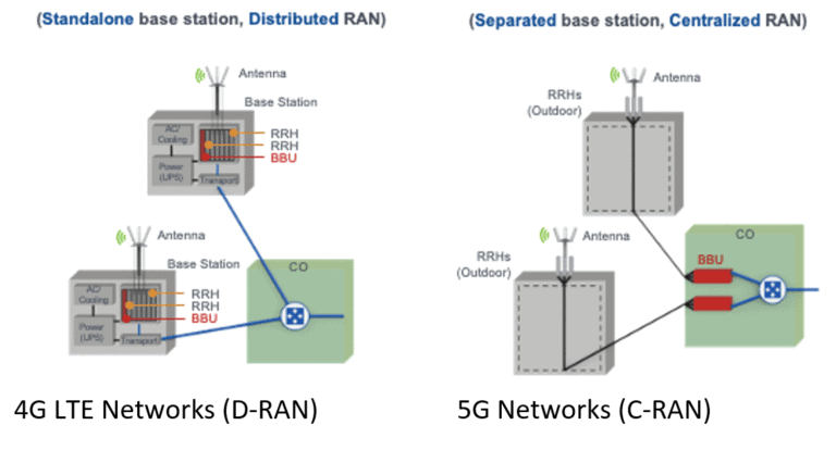
图3:4G LTE与5G网络拓扑
根据电信运营商,consumpt的力量ion of one band 5G equipment maybe 350% that of 4G with a similar configuration [6]. A 5G BBU consumes about 300W while an RRU consumes about 900W at a 30% load (peak is ~1.4 kW). As more frequency bands are added in the next 3 years, the peak power consumption will increase to about 14 kW. Beyond that, with the addition of mm-wave, the peak power may increase up to 20 kW [6]. Though existing 4G telecom power supplies are designed at -48V, these power supply units are not compatible with the 5G needs. The absolute power losses from the power supply cable in 4G system tend to be smaller as the power requirements are on the order of 1 kW. However, absolute losses for the same cable length are higher in a 5G system, resulting in a higher voltage drop along the cable. As with most power supplies, once the voltage drops below a threshold ‘low output voltage’, the power supply shuts off. To mitigate this problem, power supply designers may use an additional DC-DC converter to boost the voltage levels to around -57V for effective operation [6]. As a result, the increased power consumption of the 5G network brings challenges for the entire power supply system.
48V对半导体的影响狗万滚球官网
Consistent with the market requirements discussed above, there are significant increases in new market opportunities for semiconductor suppliers. In the automotive sector, the mild hybrid segment is approximately 1.5% to 2% of the total production today; however, by end of the decade, it is expected to grow to about 15%. Consequently, power semiconductor content per car is expected to increase approximately $75/vehicle due to the adoption of mild hybrid systems. Similarly, with the migration to 48V power net in hyper-scale and 5G data centers, the power device bill of material (BOM) is set to increase by about $40. Finally, due to 5G infrastructure deployment, both cabinet and blade power supply requirements will increase the need for power transistors. The 48V Ecosystem presents an opportunity for semiconductor suppliers to apply synergies among these application segments. From the overall new market opportunity, Figure 4 outlines the key application segments and respective growth prospects. Whether its 48V in automotive and cloud computing or -57V in 5G power supplies, the underlying assembly, and test business is also set to grow significantly in the next decade.
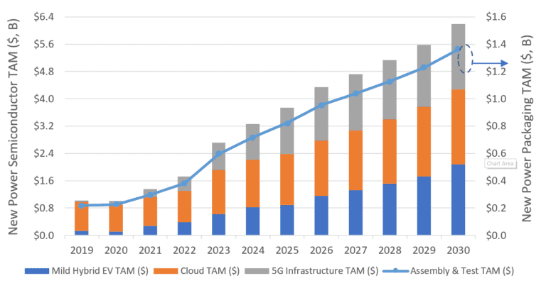
图4:48V生态系统新的可用市场(TAM)(Amkor估计)
技术Trends that Need Power Packaging
Considering the application trends discussed thus far, the common theme is that customers need power semiconductor solutions that are highly efficient, occupy less space, and very reliable. For over 30 years, power conversion efficiency and cost ($/W) has shown steady improvement due to innovations in silicon (Si) Power MOSFET technologies, power packages and circuit topologies. Though Si has been the workhorse, figures of merit (Ron x Qg, Ron x Qoss) have reached the theoretical bounds of Si. Newer material systems, such as gallium nitride (GaN), have entered the market space offering better performance. However, to realize system benefits, packaging technologies must not limit achievable electrical and thermal benefits. Historically, power device packaging has evolved from through-hole packages such as TO-247 andTO-220将长引线连接到带有引线(如D2PAK)的表面贴装组件,DPAK.,SO-8。此外,铅封装已被脱脂表面安装选项所取代,例如无侵扰(TOLL) andPQFN公司。随着需求增加的功率密度和高度可靠的解决方案,包装行业必须提供创新的选择来满足新兴趋势。客户可能需要通过双侧冷却,芯片尺度包装和多模集进行有效的热管理来解决方案,以减少寄生。但是,在成本,性能和可靠性方面将有权衡。
汽车用例提供了一个有用的例子。皮带起动器发电机的应用需要约12kW,其中电力系统的中间轨道为48V。为电机供电的逆变器级使用额定电压高于48V的MOSFET,而电流高于500A。通常,多个MOSFET并联以满足全功率要求。在功率级中,设备在高侧和低侧支腿中并联以实现完整的3相实施,印刷电路板(PCB)空间是额外的,尤其是当功率级集成在电机内部时。D2PAK如图7L,在这种应用和瓦数案件中使用的公共包装,其封装尺寸为15×10x4.4mm。但是,当功率级需要几个包装时,空间变为溢价。与D2Pak类似,Toll(11.7 x 9.9 x 2.3 mm)也是一种模制包,已针对高功率和高可靠性应用进行了优化。但TOLL(图5)提供dimens缩水30%ions and > 50% smaller form-fit allowing compact designs and high current capability and low thermal resistance (RthJC). Another critical aspect to note is evolving mission profiles for automotive semiconductors which mandates higher levels of reliability at the board level.
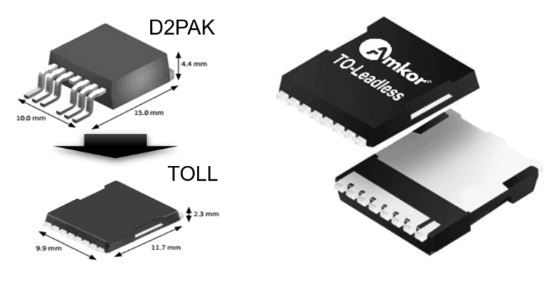
Figure 5: D2PAK 7L vs. TOLL Power Packages
云和边缘数据中心的服务器电源存在不同的电源要求,为CPU核心,DDR内存和负载点等备用轨道,风扇和驱动器提供电源。对于PORNATION的分布点(POL)架构是优选的应用,单个封装中的电源块或功率级是最佳选择。具有集成灵活性,套餐如PQFN公司(图6)越来越流行。PQFN封装提供了范围,以提高芯片封装比和暴露散热器,从而在更高的功率密度为服务器电源。更大尺寸的PQFN通过使用铜(Cu)夹技术的芯片堆叠提供多个fet(功率块)的集成,如图6中PQFN双堆叠图片所示。另一种选择是将栅极驱动器与高侧和低侧功率FET(功率级)集成,以实现DrMOS等智能功率应用。这在图6中显示为一个单堆栈选项。此外,PQFN还应用于电信基础设施、基带板和DC-DC转换器等领域。
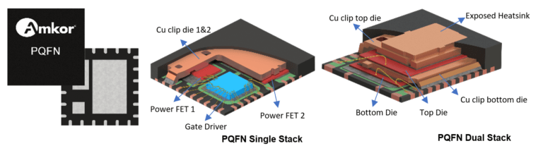
图6:PQFN多模电配置
Power Packaging Trends for the 48V Ecosystem
As one of the leading outsourced assembly and test (OSAT) suppliers, Amkor has a diverse portfolio to offer in the emerging 48V Ecosystem. This strong position stems from a global presence and partnerships with top semiconductor suppliers.Power packaging由两个不同的工厂提供支持-马来西亚阿姆库尔(ATM)和日本福井阿姆库尔(ATJ6)。广泛地说,提供了一些创造价值的功能和技术优势,如先进的引线框架技术(XDLF)、铜夹互连、铝楔键合和节省空间的表面贴装、扁平引线设计。如前所述,电源封装已经从通孔(TO)型发展到表面贴装(SMD)封装。近年来,TOLL等贴片无铅封装越来越受到人们的关注。这些封装完全符合汽车电子委员会的AEC-Q101标准,具有足够的功率循环和车载温度循环(TCoB)能力。然而,在可靠性、当前能力或封装特性方面可能会出现限制。因此,下面将讨论一些新兴的包装理念,以满足新的48V生态系统电源包装市场的要求。
Based on IPC International’s IPC-9701 standard, TOLL can fulfill the standard requirements of 1000 cycles (onboard) depending on die size and thickness. However, designers who require a high die to package ratio and/or extended reliability may find it challenging. Typical board substrates used are FR4, Cu-based intermetallic substrates (IMS), or Al-based IMS. However, when a substrate option such as Al-based IMS is considered, the board level reliability issues of TOLL may further exasperate due to vastly different thermal coefficients. The mismatch between the Cu leadframe and Al-IMS will lead to higher stress on the solder material, causing solder fatigue and cracks. By employing a gull-wing approach in the TOLL design (see Figure 7), TOLG can significantly improve the reliability levels while still offering comparable thermal and electrical performance. The flexibility of the gullwing design offers a marked improvement in reliability performance. This becomes imperative due to changing mission profiles in end-user segments, where extended stress and reliability have become a key system requirement.
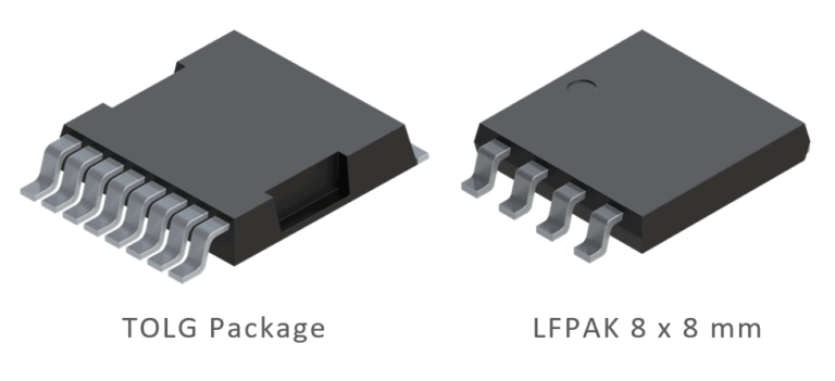
图7:Tolg和LFPAK 8 x 8 mm封装
Alternatively, as datacenter server farms migrate to 48V architectures, power density requirements to address PUE will be a key concern. The trends of improving power device figures of merit can only take designers so far. Newer packages, such as the LFPAK (see Figure 7) in bigger body sizes, like 8 x 8 mm, will be a great addition. Compared to a traditional 7L D2PAK, an 8×8-mmLFPAK机械尺寸的60%较小,但体积的80%也是如此。就互连技术而言,线键决定了当前发电电源产品的承载能力。在D2PAK的情况下,所用键合线的最大直径为20密耳。然而,在LFPAK 8 x 8 mm中,通过使用铜夹技术进行互连,电流承载能力将要高得多。通过剪辑技术显着大化来自线键的寄生电阻和电感。这种包装方法减轻了可实现的电力密度的一些问题。
在服务器架构,fast-transient反应times demanded by microprocessors have led to the adoption of POL converters and voltage regulators. The parasitic impedances of conventional power electronic packages, operating at frequencies over 1 MHz, are not adequate. In this regard, Amkor is exploring chip-scale packaging for power transistors – the PowerCSP™ package – as shown in Figure 8. This innovative concept is a leadframe-based chip-scale packaging, allowing for double-side cooling where the top/leadframe side can be connected to the heat sink or water cooling. The bottom side of the package can be mounted to the PCB using thermal vias and power Cu layers. Key advantages of the PowerCSP concept are that it eliminates wire bonds and/or Cu clips, resulting in low parasitic resistances and stray inductances thereby reducing conduction losses and switching losses, respectively. Additionally, the reduced parasitic inductance of PowerCSP helps in achieving higher switching frequencies and power densities. Compared to plastic power packages such as the PQFN or LFPAK, the PowerCSP design can be constructed with a simplified process flow thereby reducing possible sources for reliability concerns as well. Furthermore, PowerCSP packaging would provide a gateway for multi-die integration to realize converter-in-package type solutions.
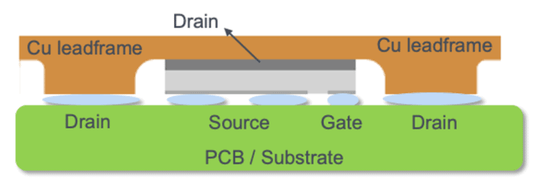
图8:PowerCSP™包概念
Summary
受环境,经济和社会因素的推动,对复杂的电力电子解决方案的需求,降低总体拥有成本,将增加。新兴的48V生态系统为功率半导体封装段提供了一种倾向的网关。狗万滚球官网虽然电力包装成熟,但需要改进以满足新兴趋势。无论是改善骰子到包装的比例,还原包装寄生剂还是增加电流携带的互连,广泛的现有产品组合和创新的新方法都可以提供解决方案。这需要强大的技术诀窍和完善的客户伙伴关系,以提供这些挑战。Amkor不仅可以满足这些要求,而且还具有金融和技术实力,为设备和设施做出重大投资,并为其汽车和其他权力客户提供长期支持。
Author:Ajay Sattu,SR Manager,汽车战略营销
参考:
[1]。Manish Menon等人,“48V架构:2018年8月14日,OEM的成本效益主张”
[2]. Automotive IQ et al, “The rise of 48V technology – an Automotive IQ eBook”, Aug 14th, 2018
[3]. Branka Vuleta et al, “How much data is created every day?”, Jan 30th, 2020
[4]. Energy Innovation et al, “How much energy do datacenters really use?”, Mar 17th, 2020
[5]。Wiwynn等人,“48V:数据中心的改进的电力输送系统”,2017年6月
[6]。全球ICT能源效率Summit等,2019年10月“5G电信电力目标网络”
PowerCSP™是Amkor Technology,I狗万注册地址nc。的商标
© 2020, Amkor Technology, Inc. All rights reserved.
相关的帖子

Increasing the Conductive Density of Packaging


Coronavirus(Covid-19)的Amkor更新